Audio frequency amplifier circuit with transistor
When various circuits are designed, I often want to make the low frequency amplification circuit of a little A class bias with a transistor. It introduces the method of designing the transistor circuit of one Koku that uses a part of grounded emitter of "Design fabrication of the AM wireless microphone" as an example.
Because the second step is a similar circuit, it omits it though the circuit introduces here is only the first step The transistor in the low frequency part in "Design fabrication of the AM wireless microphone".
A class AF amplifier design with a transistor
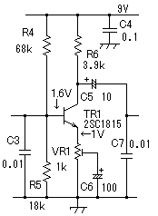
This schematic diagram amplifies signal voltage (0-10mVp-p) of the electret capacitor mike with the low frequency amplification circuit of the first step by about four times-about 80 times.
Design condition
Use transistor 2SC1815(maximum rating Vcbo=60V Ic=150mA)
Power-supply voltage Vcc = 9V
Emitter current current of Ie ≒ collector Ic≒1mA
Voltage of emitter Ve = 1V
Direct current amplification rate hfe = 100
Voltage amplification level About A =4-80
Calculation of each constant for low-frequency amplifier
The voltage of the emitter of the grounded emitter is set to 1/10-1/5 of the power-supply voltages for a steady bias. The dynamic range narrows though it comes the higher this voltage is, to stabilize. VR1 is half fixed resistance to set the gain (gain). The usage of such VR is not done because it adjusts it from gain 0 in a usual mike amplifier.
Resistance uses all things of the E12 affiliate. Most circuits can be designed by the E12 affiliate.
Calculation of VR1:
VR1 = Ve/Ie = 1V/1mA = 1kΩ
Calculation of Ib in current of base:
Ib = Ie/hfe = 1mA/100 = 0.01mA
Calculation of R5:
The current of the breeder becomes 0.1mA because it throws the current ten times Ib into the bleeder resistance of R5 for a steady bias. Because forward voltage (Vbe) between the base emitters of the transistor of A class amplification becomes about 0.6V, voltage Vb of the base.
Vb = Ve+Vbe = 1+0.6 = It becomes 1.6V
R5 = Vb/0.1mA = 1.6/0.1 = 16kΩ
Vicinity 18kΩ is used. (Of course, R5 of 15kΩ is not cared about. At that time, the value of R4 is reduced more than the calculation values.)
Calculation of R4:
It flows by 0.11mA because the current of the breeder and Ib flow to R4.
R4 = (9V-1.6V)/0.11mA ≒ 67kΩ
Vicinity 68kΩ is used. In this case, the value whose R4 is larger than the calculation value is chosen because it made it to a value that is larger than the calculation value when R5 is decided.
Calculation of R6:
Power-supply voltage Vcc = As for the output signal, the movement dynamic range becomes 8V from 9V and voltages Ve=1V of the emitter between 9V and 1V. It only has to make collector voltage Vc and to make it to the center almost, to adjust the voltage descent of R6 to 8/2=4V about the dynamic range.
R6 = 4/Ic = 4/1mA = 4kΩ
Vicinity 3.9kΩ is used.
Minimum voltage amplification level Amin.
A minimum voltage amplification level is decided when deciding that R6 is VR1. Output signal voltage (VR1e) of the emitter almost becomes equal with the signal voltage of the base because it becomes operation like grounded emitter when half fixed resistance VR1 was made the lowest gain in a word. In a word, because it is Ie≒Ic, the collector output signal voltage : It becomes R6xIc≒R6xIe
Amin. = R6/VR1 = 3.9/1 = It increases by a factor of 3.9
(Because the input resistance in the following steps also starts output R6 in parallel, do not actually become it like this accurately.)
Calculation of C6:
Impedance Ze that sees the direction of the emitter of TR1 from the outside of the emitter of TR1 becomes about 1/hfe of the harmony of impedance R1, R4 that sees the base circuit from the transistor, the shunt impedance of R5, and hie of the transistor. Hie of 2SC1815 transistor is the one of about Ic=1mA and hfe=100 and about 3kΩ.
Ze = {(R1//R4//R5) + hie}/hfe = It becomes {(2.2k//68k//15k) +3kΩ}/100≒ 49Ω
(R1//R4//R5)It is assumed the one to show the resistance of the parallel circuit of peel R1, R4, and R5
Because the capacitor of impedance that is lower than this is necessary as C6, C6=100μF that becomes impedance 8Ω200Hz of the lowest frequency is used.
Maximum voltage amplification level Amax.
When it becomes the shunt impedance of the input impedance of R6 and the next steps and about 8kΩ of RL is this here
RL = It becomes R6//8kΩ≒2.6kΩ.
Amax. = (hfe×RL)/hie = (100×2.6kΩ)/3kΩ ≒87 times
It near actually becomes small than the calculation value.
Decision of C4, C5, and C7:
C4 is for the by-pass of the high frequency of chiefly 700 the kHz, and impedance by 700kHz is 2.3Ω because it uses this low frequency amplification circuit for the AM transmitter. It installs it in a place near TR1 as much as possible.
To become impedance that is 200Hz very lower than output impedance 3.9kΩ of this steps with the coupling capacitor of the signal, C5 is selected. 10μF is used.
C7 prevents the high frequency from entering the high region cutting of the voice frequency and the base circuit of TR2. To become the impedance of improving 4kHz a little compared with parallel resistance about 2.6kΩ with the input resistance in R6 and the next steps, 0.01μF is selected.